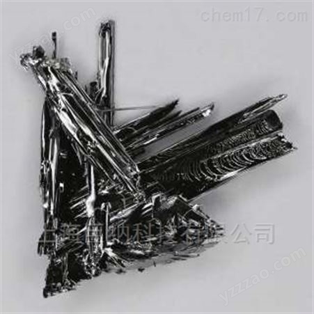
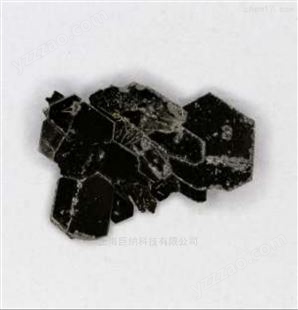
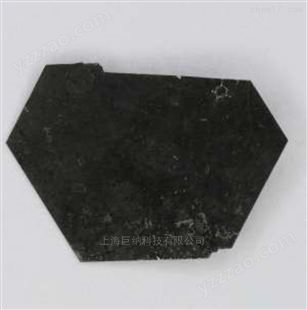
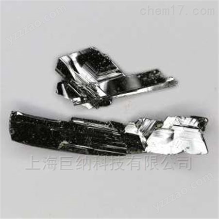
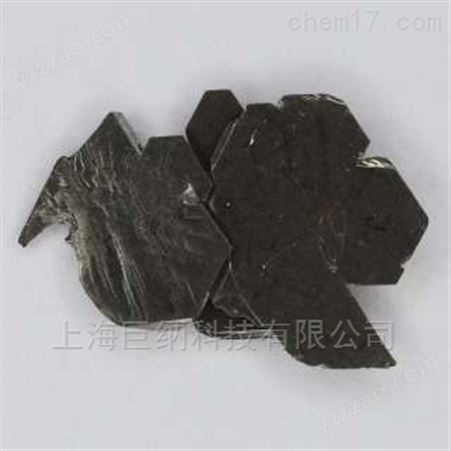
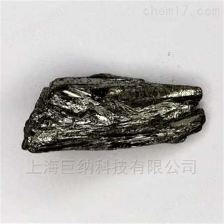
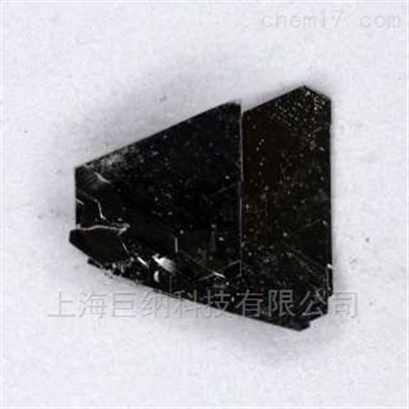
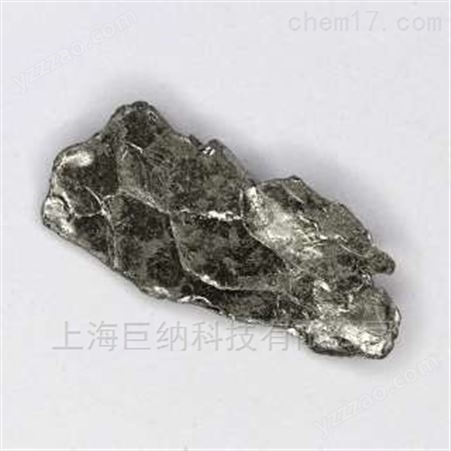
Platinum ditelluride (PtTe2) is a member of transition metal dichalcogenide (TMDCs) family with the MX2 formula. In the bulk form, it is an established metal with complex band structure, in the monolayer it is arguably both semiconductor with band gap value in the far IR or metallic (J. Phys. C: Solid State Phys. 19, 995).
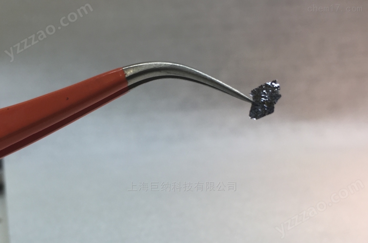
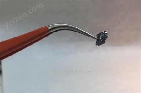
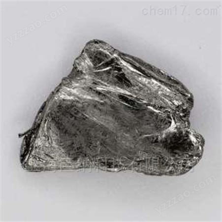
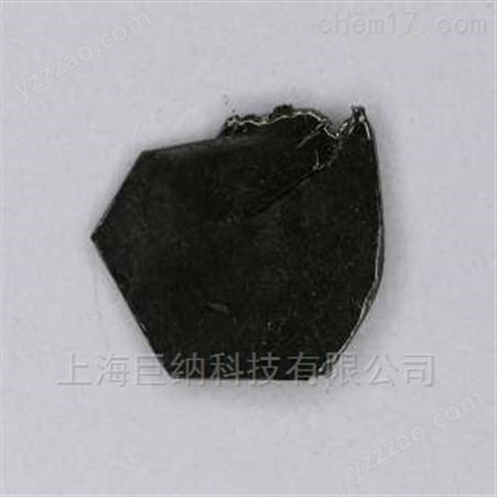
As they are semiconductor grade and highly crystalline, you do not need to worry about amorphous phase, defects, or contamination. The crystal size is very large in size and they are perfectly layered in the 001 direction (c-axis - see XRD pattern-) and thus it is very easy to exfoliate and yield monolayers up to 100& yield rate. Single domain size is much larger than 50 microns which enables you to yield large monolayer areas.
The crystals were measured and confirmed by x-ray diffraction (XRD), x-ray photoelectron spectroscopy, Raman, SIMS, and Auger electron spectroscopy techniques.
4 years of growth optimization : In these 4 years, we have perfected our PtTe₂ growth to fit to your needs. We offer perfect stoichiometry (no other hidden phases), no amorphous regions, superior domain sizes yielding large monolayers, Our crystals have impressive semiconductor purity levels (99.9995 or higher) to bring you highest quality materials at large sizes.
Growth method matters> Flux zone or CVT growth method? Contamination of halides and point defects in layered crystals are well known cause for their reduced electronic mobility, poor e-h recombination, low-PL emission, and lower optical absorption. Flux zone technique is a halide free technique used for synthesizing truly semiconductor grade vdW crystals. This method distinguishes itself from chemical vapor transport (CVT) technique in the following regard: CVT is a quick (~2 weeks) growth method but exhibits poor crystalline quality and the defect concentration reaches to 1E11 to 1E12 cm-2 range. In contrast, flux method takes long (~3 months) growth time, but ensures slow crystallization for perfect atomic structuring, and impurity free crystal growth with defect concentration as low as 1E9 - 1E10 cm-2. So if your research needs truly high quality crystals for optoelectronics, scanning tunneling microscopy, spectroscopy, and other projects that rely on defect free crystals, flux zone growth is ideal for you. However, if you need catalytic materials presence of defects typically helps and in such case CVT method is better suited. During check out just state which type of growth process is preferred. Unless otherwise stated, 2Dsemiconductors ships Flux zone crystals as a default choice.

所有评论仅代表网友意见,与本站立场无关。